FPGA Design
We use the FPGA to drive the display output to the 64 x 64 LED matrix. We implemented SPI so our FPGA can communicate with the MCU. Because the 64 x 64 LED matrix only supports three bits of colors by default, we had to PWM the display so that we could achieve a wider range of colors. We implemented Binary Coded Modulation, allowing for 12 bits of color in our final design (4096 colors, compared to the default 8). In addition, our FPGA diplay is buffered, as we store the entire display’s contents into SPRAM, preventing visual glitches.
The FPGA also serves as a physics accelerator for our MCU, so we can speed up the calculations. The FPGA is responsible for the core physics simulation and display control. The original plan was to store the simulation in Block RAM, but we were unable to get that working before our final iteration, so ended up storing our simulation in the onboard LUTs.
More information and specific implementation details can be found in our GitHub repository
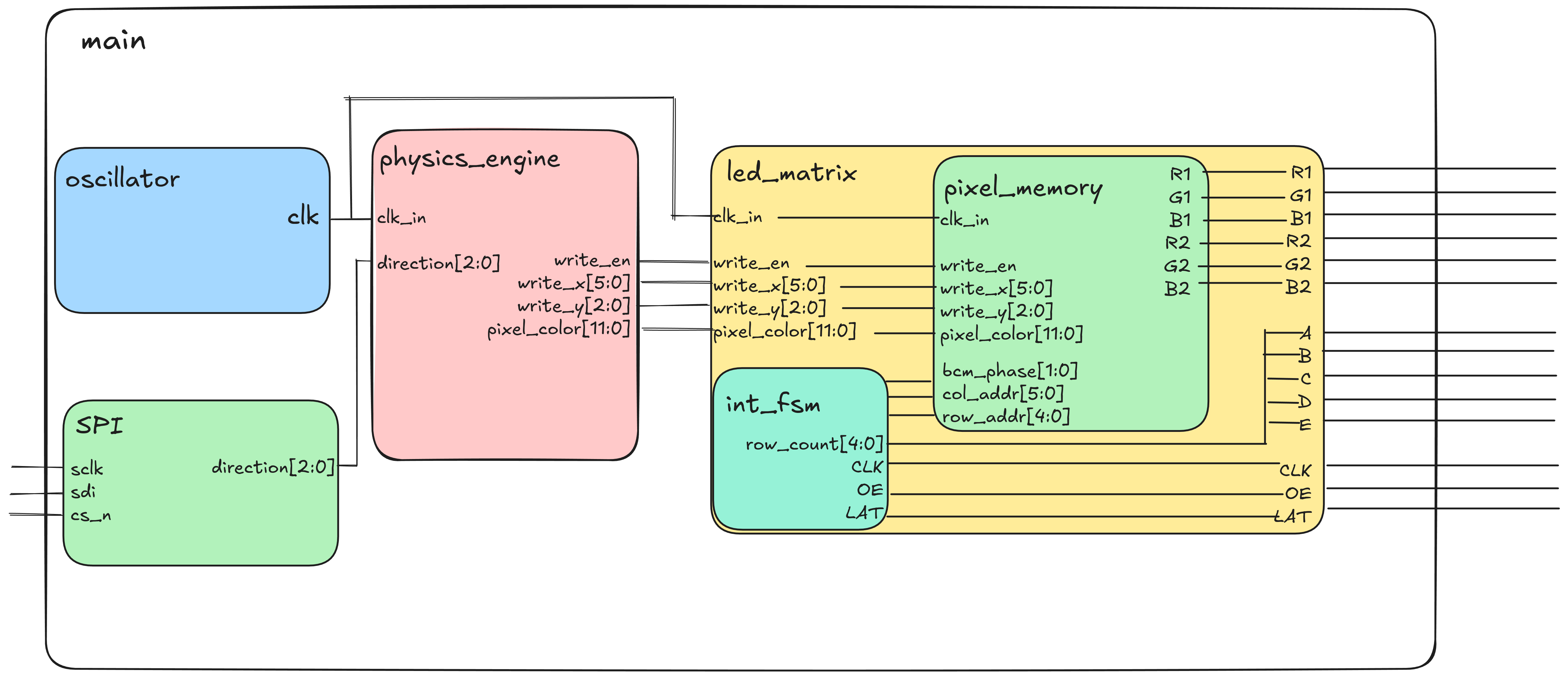
Block Diagram
Here is a Block Diagram demonstrating our implementation on the FPGA.

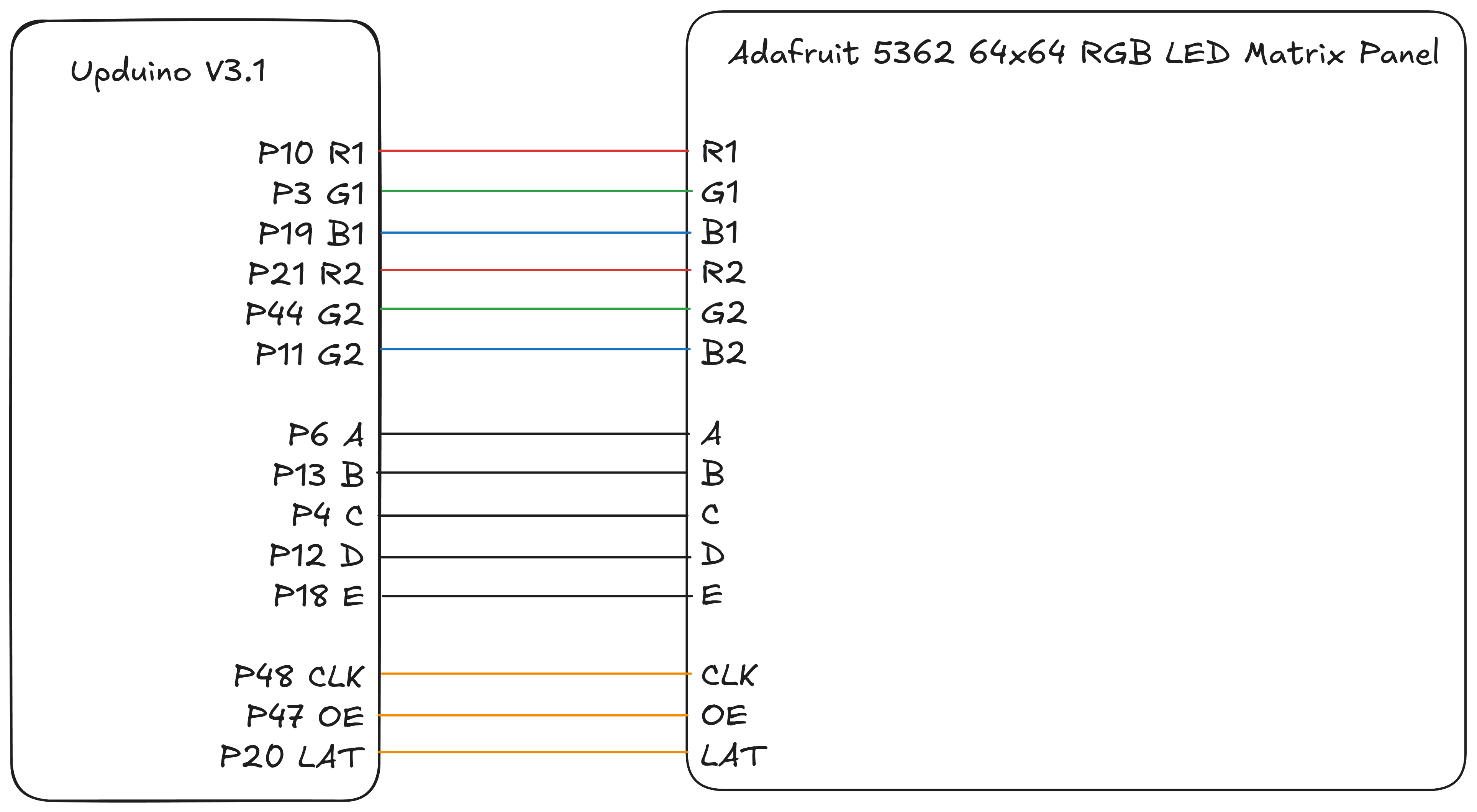
Schematic
And here is a schematic showing our connections directly with the 64x64 LED Matrix when we were writing the Display driver.

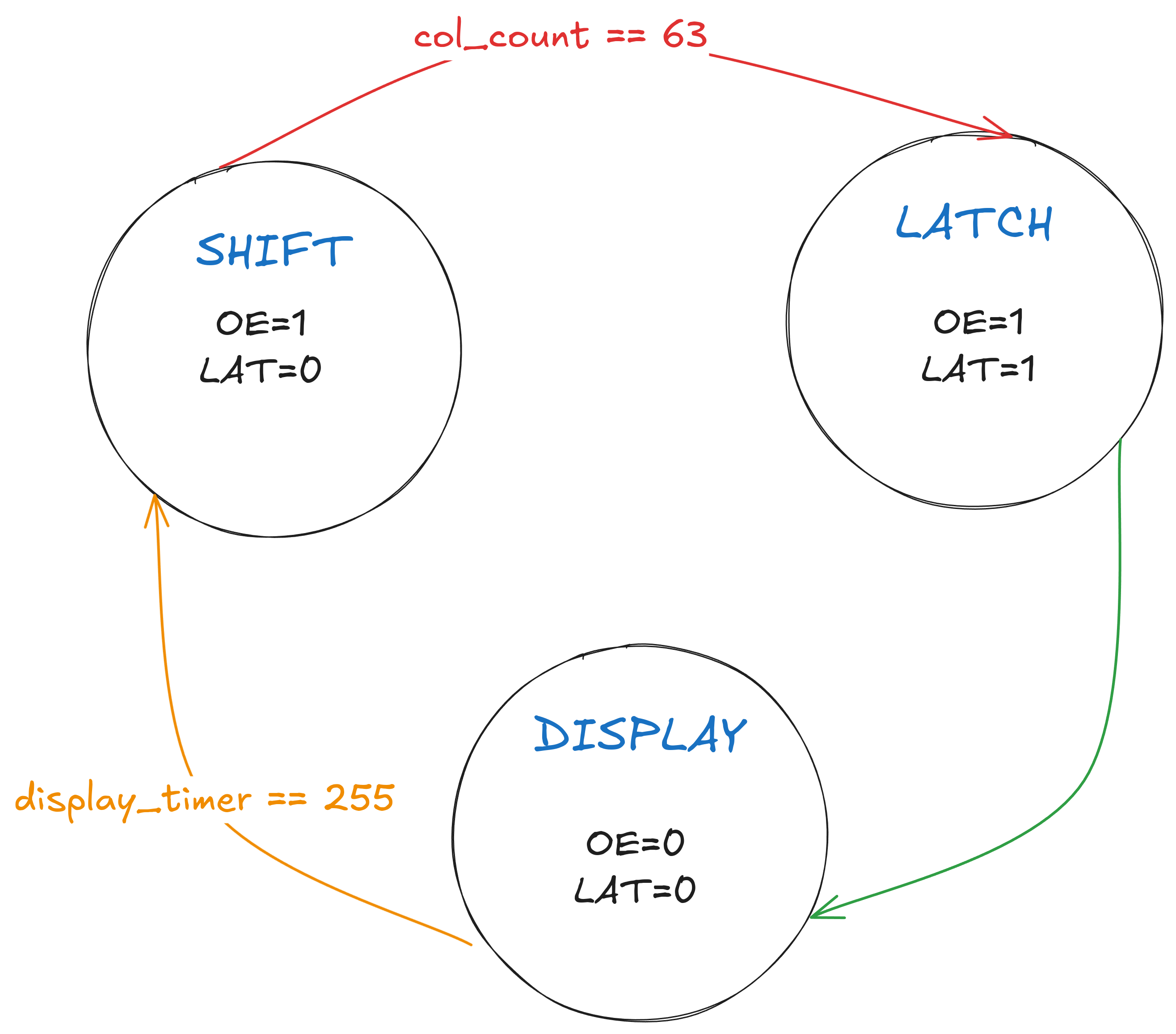
State Machine
Below is the diagram of the state machine used for lighting up the display.

The SHIFT state basically iterates over all of the columns and shifts the pixel colors into the PIXEL display, while the LATCH state just sends a signal to the 64x64 LED Matrix to indicate that it’s been written to, and the DISPLAY state enables the (active-low) OE bit so that the output is actually put onto the matrix.